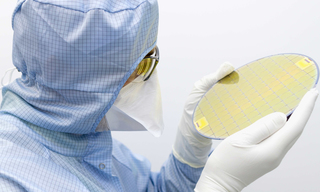
Defect Inspection
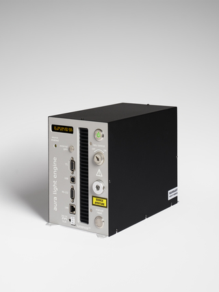
Advancing Semiconductor Defect Inspection: Harnessing the Precision of LEDs and Lasers
In semiconductor defect inspection, the choice between LEDs and lasers depends on the specific requirements of the inspection task, such as resolution, sensitivity, and the type of defects being targeted. Both light sources offer advantages and are used in complementary ways to ensure thorough and accurate defect inspection in semiconductor manufacturing.
LEDs in Semiconductor Defect Inspection
- Uniform Illumination: LEDs provide uniform and consistent illumination, which is essential for detecting defects on semiconductor wafers. The uniformity of LED illumination helps ensure that defects are not missed due to uneven lighting.
- Wavelength Selection: LEDs can emit light at specific wavelengths, allowing inspectors to tailor the illumination to enhance the visibility of certain types of defects. Different materials and defects may be more visible under certain wavelengths of light.
- Energy Efficiency: LEDs are energy-efficient, consuming less power compared to traditional light sources. This is beneficial for reducing the operating costs of defect inspection systems, especially in high-volume manufacturing environments.
- Longevity: LEDs have a long operational life, reducing the need for frequent replacement and maintenance. This improves the reliability and uptime of defect inspection systems.
Lasers in Semiconductor Defect Inspection
- High Resolution Imaging: Lasers can be used in scanning microscopy techniques to provide high-resolution images of semiconductor surfaces. This allows inspectors to detect and analyze defects at a very fine scale.
- Non-destructive Inspection: Laser-based inspection techniques are often non-destructive, allowing for the inspection of delicate semiconductor materials without causing damage.
- Defect Localization: Lasers can be used to precisely localize defects on semiconductor wafers, providing valuable information for process optimization and defect mitigation.
- Surface Profiling: Lasers can be used for surface profiling to detect variations in surface height or roughness, which can be indicative of defects or process issues.
In semiconductor defect inspection, the choice between LEDs and lasers depends on the specific requirements of the inspection task, such as resolution, sensitivity, and the type of defects being targeted. Both light sources offer advantages and are used in complementary ways to ensure thorough and accurate defect inspection in semiconductor manufacturing.